Clik here to view.
Silicon and carbon are reluctant partners. Although the two elements are among the most abundant on Earth, they almost never bond in nature and it takes a lot of heat and pressure in the lab to coax them into working with each other. But when they do stick together and form a material called silicon carbide (SiC), it’s something to see.
“SiC is a key building block for next-generation devices,” says Danielle Merfeld, global technology director at GE Global Research. “It takes features from diamond, one of the toughest materials in the world, and combines them with features of silicon, our ubiquitous semiconductor technology in electronics, and takes the best of those to make a very new kind of material for power electronics. SiC can more efficiently handle higher voltages and three times the amount of energy compared to silicon chips. Suddenly, you can run everything from locomotives to planes and wind farms faster, hotter and more efficiently.”
For example, retrofitting a datacenter with SiC chips would make it 5 percent more efficient. The technology could allow aircraft makers to shed 1,000 pounds from a passenger jet, reduce the weight of a locomotive by 5 percent, cut power losses inside wind and solar inverters by half, and make hybrid electric vehicles consume 10 percent less fuel.
GE – together with the SUNY Polytechnic Institute’s Colleges of Nanoscale Science and Engineering, the New York State and other industry partners – is now building a new SiC foundry in Utica, N.Y. The company, which has been working on SiC for almost 25 years, also contributed intellectual property valued at $100 million to get the project on its way.
GE Reports recently visited Merfeld’s GRC lab. Take a look.
Image may be NSFW.
Clik here to view. GE started working with SiC in 1991. The first product was a hardy UV photodiode that could withstand the infernal heat inside a gas turbine and monitor the flame. The latest products include power electronics that can handle the hot and harsh environment inside oil wells, aboard planes and ships, and under the hood of hybrid electric cars.
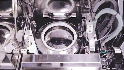
Manufacturing a silicon carbide chip requires over 200 steps performed in a clean room, and companies have to negotiate pitfalls opened by the complicated interactions between silicon, carbon and metal oxides. The images above and in the top GIF show one of the first fabrication steps: using spin coating to deposit a thin layer of photoresist that allows workers to pattern the wafer.
Image may be NSFW.
Clik here to view. The very first SiC application a century ago was as an abrasive. Today, the material’s hardy constitution gives SiC chips excellent reliability and potential lifespans of 100 years. This comes handy in deep-sea oil wells or offshore wind turbines, which must perform without a hitch for long periods of time.
Image may be NSFW.
Clik here to view. The New York foundry will manufacture SiC chips on 6-inch wafers with more than double the wafer area, compared to standard 4-inch technology. The larger size will help cut costs and scale production. The GIFs above show microscopes inspecting chips on an SiC wafer.
Image may be NSFW.
Clik here to view. GE makes SiC chips called MOSFETs – metal-oxide semiconductor field effect transistors. They help manage power inside machines and can handle temperatures as high as 200 degrees Celsius (392 Fahrenheit), where ordinary silicon would fail. Above is a partially processed 6-inch wafer in the early stages of patterning.
Image may be NSFW.
Clik here to view. An SiC wafer like this one can hold hundreds of chips. They can handle over 1,000 volts and up to 100 amps. The picture above shows a finished wafer with individual MOSFET chips.
Image may be NSFW.
Clik here to view. A close up view of a power module – in teal – showing three SiC MOSFETs with their power and signaling connections. The module is a key building block for power electronics systems. It processes raw electrical power into clean sine waves that customers can use.
Image may be NSFW.
Clik here to view. Image may be NSFW.
Clik here to view. GE engineers are working with two flavors of SiC power modules. Unlike the teal power module with its silver wire bond connections, the yellow module above has no wire bonds. “The SiC MOSFET is a high-performance device,” says Ljubisa Stevanovic, advanced technology leader at GE Global Research. “In an automotive analogy, it’s a racecar engine that’s much faster than conventional devices. The teal module shows the sturdy, conventional design that’s built like a pickup truck. But the yellow module above has no wire bonds. It’s like a Formula 1 chassis. It really allows us to go fast.”
Image may be NSFW.
Clik here to view. “In applications requiring high speed we use SiC modules without wire bonds, which deliver amazing performance,” Stevanovic says. The golden rectangles are transistors and the silver squares are diodes.
Image may be NSFW.
Clik here to view. This SiC Power Block sports several SiC modules, including electronic controls, energy storage and cooling components. Engineers can use the device to manage power for a wide range of applications. “The SiC Power Block delivers maximum power in the smallest, most efficient package and this self-contained and fully optimized unit can manage power inside wind and solar farms, locomotives, datacenters and many other applications,” Stevanovic says. “This is the perfect example of the GE Store. The standard power block can be applied for different systems across GE. It makes the application engineer’s job easier. They don’t have to reinvent the wheel every time they want to use SiC.”